---
title: "Running Mainline Linux and a 13-LED Light Show on an Old MyRepublic Fiber ONT"
date: 2026-11-07
description: "After renewing my MyRepublic fiber contract, they didn't want the old Nokia G-240G-E ONT back. Naturally, I wrote a custom bootloader, ported mainline Linux 7.4-rc1, and turned its 13 front-panel LEDs into a button-toggled light show."
author: "Daan van Gorkum"
url: "https://dj.vg/posts/nokia-g-240g-e-ont-bootloader-mainline-linux/"
markdown_url: "https://dj.vg/posts/nokia-g-240g-e-ont-bootloader-mainline-linux/index.md"
tags: ["hardware", "reverse-engineering", "embedded", "linux", "mips"]
reading_time: "14 min read"
---
# Running Mainline Linux and a 13-LED Light Show on an Old MyRepublic Fiber ONT
When I renewed my MyRepublic fiber subscription here in Singapore recently, they sent over new gear and told me they didn't need the old **Nokia G-240G-E** Optical Network Terminal (ONT) back. It simply wasn't worth collecting.
So the box ended up sitting on my desk.
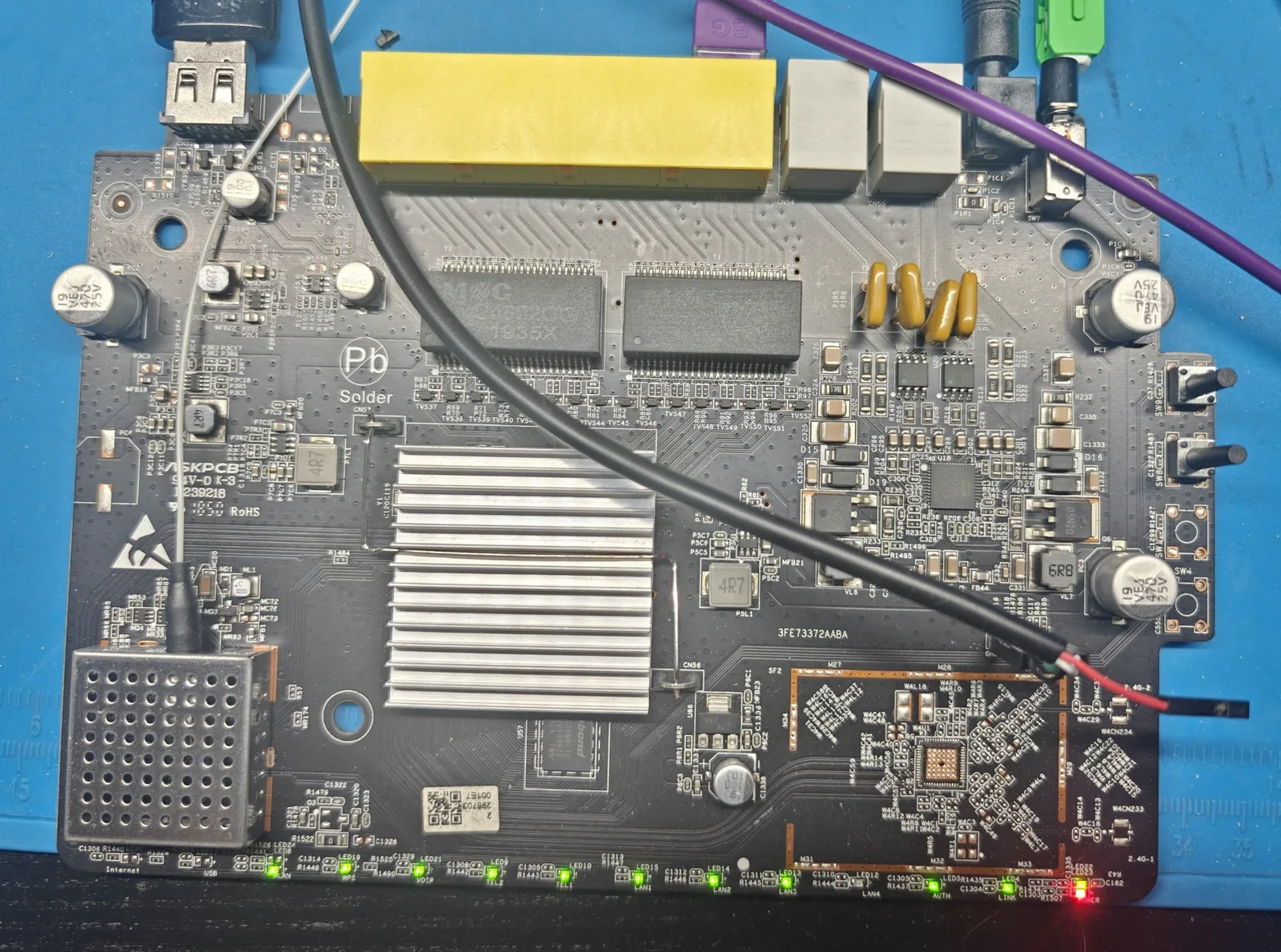
The bare PCB of the Nokia G-240G-E ONT (board silkscreen 3FE73372AABA / assembly 3FE46918AAAA): silver heatsink over the EcoNet EN751221 SoC, Winbond DDR3 memory right below it, shielded GPON BOSA stage on the bottom-left, unpopulated Wi-Fi footprint on the bottom-right, and the row of front-panel LEDs glowing along the bottom edge.
Let's get the obvious question out of the way first: is there any practical reason to repurpose an old carrier GPON ONT in 2026? Not really. A cheap ARM SBC or mini-PC is much faster, uses less power, and doesn't have half its silicon dedicated to ISP fiber termination and analog telephone lines.
This project was purely a "just because I can" rabbit hole. I had a locked-down piece of ISP hardware that nobody wanted back, a row of **13 individual status LEDs** along the front edge, and a physical push button on the side labeled `LED`. Making it boot a custom bootloader, run modern mainline Linux 7.4-rc1 from a USB stick, and put on a light show when you press the button sounded like a fun way to spend a few evenings.
If you want all the low-level register maps, device trees, kernel patches, and bootloader source code without the story, everything is in the GitHub repo at **[https://l.dj.vg/ont-code](https://l.dj.vg/ont-code)**.
---
## What's Inside the Box
Popping open the plastic shell reveals a surprisingly capable board (`3FE46918AAAA` in Nokia's inventory data, silkscreened `3FE73372AABA` on the PCB):
- **SoC**: EcoNet (now MediaTek / Airoha) **EN751221**, a dual-core MIPS 34Kc processor (2 VPEs / 2 CPUs) running at 900 MHz.
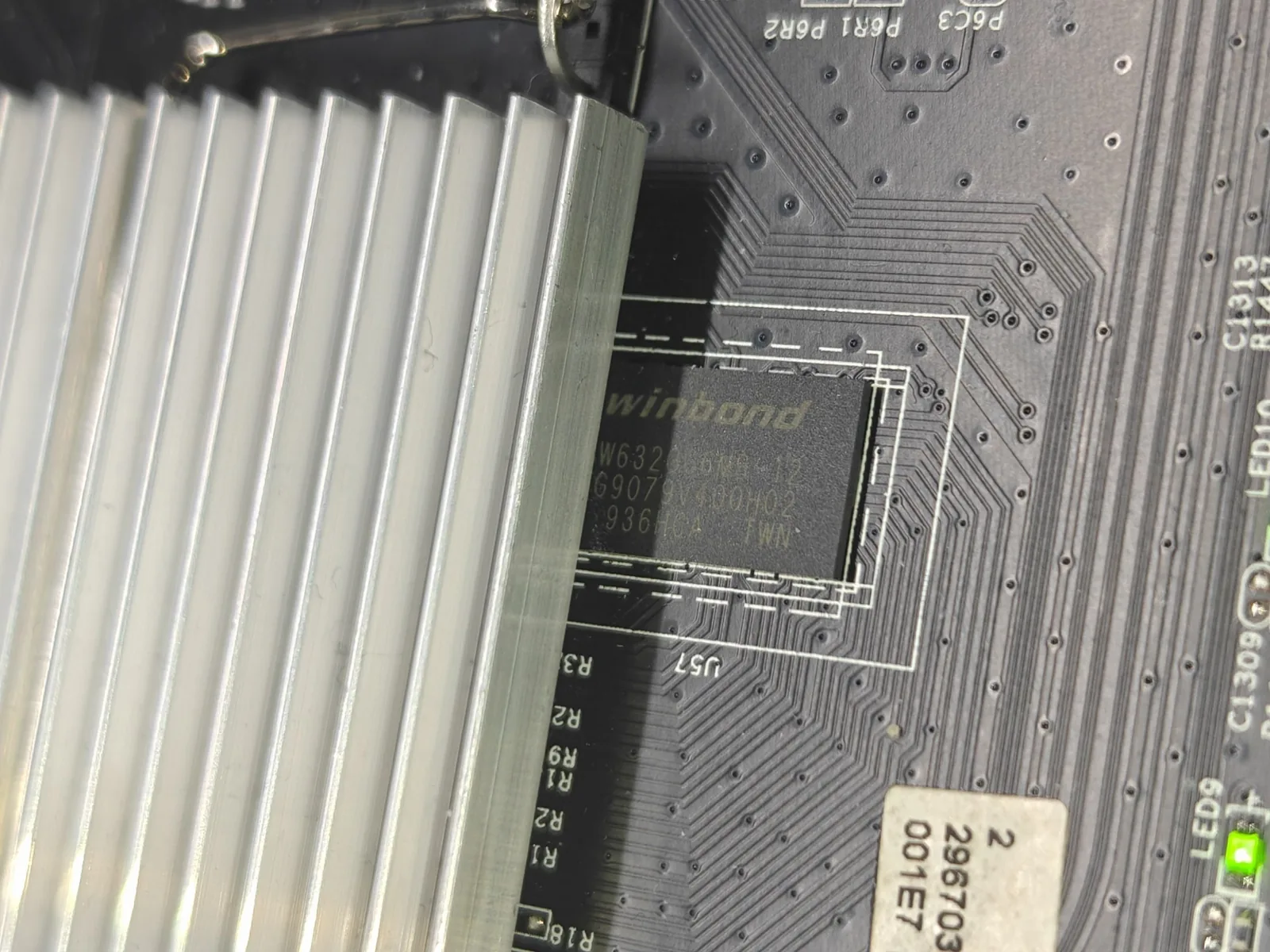
- **RAM**: 256 MB Winbond `W632GU6MB-12` DDR3 SDRAM (`U57`).
- **Flash**: 128 MB Macronix `MX35LF1GE4AB` SPI-NAND.
- **Switch**: MediaTek **MT7530** 5-port Gigabit Ethernet switch packaged inside the same Multi-Chip Module (MCM) as the SoC.
- **Optics & Voice**: Semtech `GN25L98` GPON BOSA laser/receiver stage under the metal shield, plus a Zarlink `LE9652` Dual-FXS SLIC driving the two RJ-11 phone ports.
- **Ports & UI**: 4 Gigabit LAN ports, 2 RJ-11 ports, 1 USB host port, 13 controllable LED channels along the bottom edge, and two populated side push buttons (`WPS` and `LED`, next to two unpopulated footprints on the PCB).
Close-up of the Winbond W632GU6MB-12 256 MB DDR3 SDRAM chip (U57) right beside the aluminum heatsink covering the EcoNet EN751221 SoC.
---
## Serial Console, Flash Layout, and QEMU
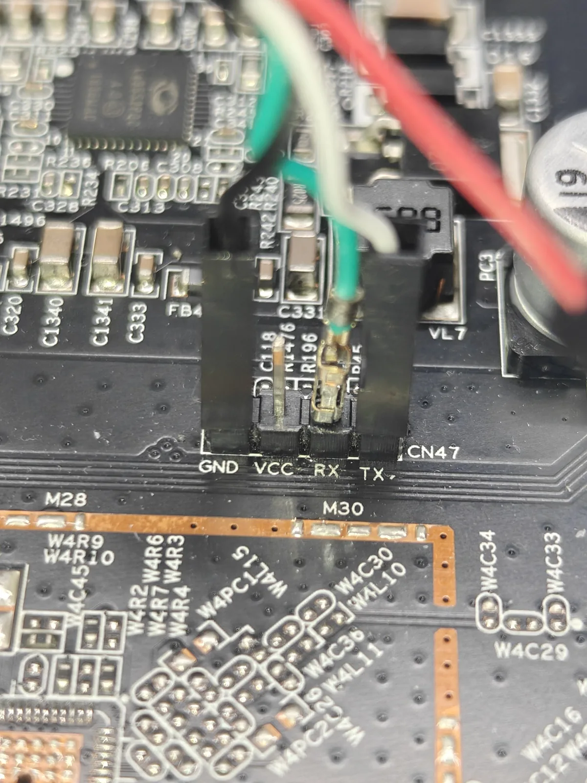
Near the right edge of the PCB sits a 4-pin header (`CN47`) with the pinout printed right on the silkscreen: `GND`, `VCC`, `RX`, and `TX`.
The 4-pin 3.3V UART header (CN47) with the pinout printed right on the silkscreen from left to right: GND (Pin 1, square pad), VCC (Pin 2, bare pin left unconnected), RX (Pin 3), and TX (Pin 4).
Hooking up `GND`, `RX`, and `TX` (while leaving `VCC` disconnected) to a 3.3V USB-to-serial adapter at `115200 8N1` gives us the boot output from EcoNet's two-stage `tcboot` bootloader:
```text
7512DRAMC V1.2.2
DDR3-1066 MHz OK
Press any key in 3 secs to enter boot command mode.
bldr>
```
Pressing a key drops into `bldr>`, EcoNet's bare-metal monitor (originally inherited from TrendChip). There is no U-Boot on this board, no network stack, and no `tftp` or `dhcp` support. What it *does* have is a basic `xmdm` command to upload bytes into RAM over 115200-baud XMODEM and a `go` command to jump to an address.
Dumping the 128 MB SPI-NAND flash and dissecting `tcboot` in Ghidra showed a classic ISP dual-bank partition layout:
| MTD Partition | Flash Offset | Size | Purpose |
| :--- | :--- | :--- | :--- |
| `/dev/mtd0` (`bootloader`) | `0x00000000` | 256 KB | Stage 1 SPL + LZMA-compressed Stage 2 (`tcboot`) |
| `/dev/mtd1` (`romfile`) | `0x00040000` | 256 KB | Factory configuration XML |
| `/dev/mtd2` (`kernel`) | `0x00080000` | 3 MB | Primary Kernel (Bank 0) |
| `/dev/mtd3` (`rootfs`) | `0x00380000` | 31 MB | Primary Rootfs SquashFS (Bank 0) |
| `/dev/mtd4` (`kernel_slave`) | `0x02280000` | 8 MB | Backup Kernel (Bank 1) |
| `/dev/mtd5` (`rootfs_slave`) | `0x02a80000` | 26 MB | Backup Rootfs (Bank 1) |
| `/dev/mtd12` (`flag`) | `0x06dc0000` | 256 KB | Active boot bank flag (`0` = Bank 0, `1` = Bank 1) |
| `/dev/mtd14` (`ri`) | `0x06e40000` | 256 KB | Nokia Resource Inventory (MAC address, serial, `3FE46918AAAA`) |
### Testing in QEMU First
Before running custom MIPS assembly on the physical board, I built a custom **QEMU machine model** (`-M en751221`) that emulates the EN751221 memory map, the 64 KB scratchpad SRAM at `0x1FA30000`, the 40-line VEIC interrupt controller, the UART, the SPI-NAND manual FIFO interface, and the QDMA Ethernet rings.
Having the QEMU model meant I could write and debug early boot code, test SPI-NAND Bad Block Management Table (BMT) parsing, and verify LZMA decompression in a virtual sandbox before ever touching the real board. Even better, once ready for hardware testing, the stock `bldr>` `xmdm` command let me chainload new bootloader builds directly into DDR3 RAM at `0x80002000` in about 4 seconds without writing a single byte to flash.
---
## Writing "Daan's Big Fat Bootloader" (and 1.5s HTTP Boot)
Uploading a 55 KB bootloader over 115200-baud serial takes 4 seconds, which is fine. Uploading a multi-megabyte Linux kernel over 115200-baud serial takes over 10 minutes, which gets old very fast when you are iterating on kernel drivers.
To fix that, I wrote a standalone bare-metal bootloader from scratch in C and MIPS32r2 assembly (**"Daan's big fat bootloader"**). Instead of bothering with UDP/TFTP, I wrote a small bare-metal driver for the EN751221's QDMA Frame Engine and embedded MT7530 Gigabit switch, added a minimal ARP + DHCP + TCP client, and implemented **`httpboot`**.
When the bootloader starts, it grabs an IP via DHCP and streams `vmlinux.bin` straight over Gigabit Ethernet from a standard Python `http.server` into RAM in **1.5 seconds**.
### Using All 13 LEDs as a Hardware Progress Bar
Streaming a kernel in 1.5 seconds is nice on the serial console, but we have 13 LEDs sitting right on the front edge of the board. I wired all 13 of them (both the direct SoC GPIO LEDs and the four `LAN1..LAN4` LEDs connected to the MT7530 switch die) into the bootloader:
The 13 front-panel LEDs (12 green + 1 red at POWER) cycling through the 9-pattern light show on the bare PCB.Close-up of the SMD LED row along the bottom edge of the PCB: an unpopulated USB pad (LED17) on the far left, followed by WLAN, WPS, VOIP, TEL2, TEL1, LAN1..LAN4 (with LAN3 lit green), AUTH, LINK, and the vertically stacked LED22 (green) + LED23 (red, lit) dies above POWER.
- **Phase 1 (Loading from HTTP or SPI-NAND Flash)**: The 13 LEDs fill up progressively from left (`WLAN`) to right (`POWER`) as the kernel image is read into memory.
- **Phase 2 (LZMA Decompression)**: While the kernel is uncompressed into `0x80002000`, an inverted dark notch sweeps across the lit LED bar so you can watch the decompression progress in real time.
- **Interactive Light Show (`ledfun`)**: Typing `ledfun` at the bootloader prompt runs a 9-pattern animation loop (a 2-LED Knight Rider scanner, center bounce, marquee wave, Tetris stack-and-drop, particle collider shockwave, and accelerating turbine spin).
---
## Chainloading from the Backup Partition (`/dev/mtd4`)
Once both the bootloader and our custom Linux 7.4-rc1 kernel were working over HTTP boot, I wanted the ONT to cold-boot into Linux automatically when flipped on.
Overwriting `/dev/mtd0` (the primary bootloader partition) carries the obvious risk of bricking the board if anything goes wrong. Using the backup kernel slot (`/dev/mtd4`, selected by setting the boot flag in `/dev/mtd12` to `1`) avoids touching `/dev/mtd0` or the stock primary firmware in Bank 0 (`/dev/mtd2` and `/dev/mtd3`).
There was one catch when we first tried putting our compressed `Linux 7.4.0-rc1` image directly into `/dev/mtd4`: the stock `tcboot` in `/dev/mtd0` printed `linux.bin image too big` and refused to boot it. Reverse-engineering `tcboot` showed why: its LZMA decompressor places its heap at `0x80750000`, which leaves a hard limit of 7.3 MB for the uncompressed image. Our modern `Linux 7.4.0-rc1` kernel uncompresses to 9.66 MB.
Fortunately, `/dev/mtd4` (`kernel_slave`) is **8 MB** wide (`0x02280000` to `0x02a80000`). That let us set up a clean two-step chainload inside `/dev/mtd4` itself:
```text
+----------------------------------------------------------------------------+
| /dev/mtd0: Factory SPL & tcboot (Untouched) |
+----------------------------------------------------------------------------+
| Bank 0 (Stock Firmware - Untouched): |
| /dev/mtd2: Stock Factory Kernel |
| /dev/mtd3: Stock Factory Rootfs |
+----------------------------------------------------------------------------+
| Bank 1 (/dev/mtd4 - 8 MB Backup Kernel Partition): |
| 0x02280000 (+0x000000): "Daan's Big Fat Bootloader" (24 KB 2RDH image) |
| 0x02300000 (+0x080000): Mainline Linux 7.4.0-rc1 (3.0 MB 2RDH image) |
+----------------------------------------------------------------------------+
| /dev/mtd12 / mtd13: Dual-Boot Active Bank Flags (set to Bank 1) |
+----------------------------------------------------------------------------+
```
On cold power-on:
1. Stock `tcboot` in `/dev/mtd0` sees Bank 1 active, loads our tiny 24 KB bootloader from `0x02280000` (which uncompresses to just 54 KB, well under the 7.3 MB ceiling), and jumps to it.
2. **"Daan's big fat bootloader"** starts up, runs a 3-second countdown, and then automatically loads `Linux 7.4.0-rc1` from `0x02300000` (512 KB further down inside `/dev/mtd4`), driving the 13-LED progress bar during both the flash read and the 9.66 MB LZMA decompression.
---
## Three Quirky Hardware Bugs Along the Way
Porting mainline **Linux 7.4-rc1** to the board uncovered a few fun hardware quirks. The full register-level details and patches are in the [GitHub repository](https://l.dj.vg/ont-code), but here is the short version of three of the most interesting ones:
### 1. The Power LED "Pinmux Knock"
Above the `POWER` label on the bottom-right of the PCB sit two stacked SMD LEDs: `LED22` (Green, on GPIO 7) and `LED23` (Red, on GPIO 23). Toggling GPIO 23 lit the red LED right away, but driving GPIO 7 high did nothing at all.
Digging into the SoC's ChipSCU registers (`0x1fa20104` and `0x1fa20108`) showed that GPIO 7 defaults to a hardware PON optical status override after reset. Until software clears bits `[6:3]` in `0x1fa20104` and sets the GPIO routing mask in `0x1fa20108`, the GPIO controller isn't actually connected to the physical pad. Once unlocked, both green (`LED22`) and red (`LED23`) can be controlled independently.
### 2. The MT7530 Switch MDIO Read Quirk
The Gigabit switch on this board is a separate MT7530 silicon die inside the SoC package, reached through a memory-mapped MDIO bridge register (`MT7531_PHY_IAC` at `0x1fb5f01c`). When bringing up the mainline `mt7530-mmio` DSA driver, physical link lights on the RJ-45 jacks came on, but Linux reported `lan1..lan4` as down.
It turned out that polling bit 31 (`PHY_ACS_ST`, busy) in `0x1fb5f01c` until it cleared and then performing a *second* register read to extract the 16-bit PHY data returned stale values on the EN751221. Capturing the register value directly from the final poll iteration fixed MDIO reads immediately and brought all four Gigabit LAN ports up.
### 3. The Serial Cable Strap Pin Trap (1,024 False Bad Blocks)
When we first booted Linux 7.4-rc1 with the SPI-NAND driver enabled, the kernel detected the Macronix flash chip and then printed `Bad eraseblock` for every single block from `0` to `1023`. Yet reading the flash from the bootloader showed zero bad blocks.
The culprit was our serial cable on `CN47`. Having a UART adapter connected during cold power-on subtly pulls `UART_TXD`, which shares a bootstrap pin sampled by the SPI controller (`SFC_STRAP` at `0x1fa10114`). When that strap bit latches low at power-on, the controller boots into a reserved mode where its DMA engine returns `0x00` for out-of-band (OOB) spare bytes. Because Linux MTD checks OOB byte 0 (`0xFF` = good, `0x00` = factory bad), it marked the entire flash chip bad. Switching the driver (`spi-airoha-snfi.c`) to manual FIFO mode (`dma_enable = false`) and single-wire SPI RX (`spi-rx-bus-width = <1>`) bypassed the broken DMA path and all 16 MTD partitions mounted cleanly.
---
## Booting Mainline Linux 7.4-rc1 and Wiring the `LED` Button
With SMP multi-threading (2 CPUs), Gigabit Ethernet (`eth0` + `lan1..lan4`), SPI-NAND (`/dev/mtd0..mtd15`), USB (`xhci-mtk`), Watchdog, I2C, Crypto, xPON, and VoIP drivers all working in **Linux 7.4.0-rc1**, I plugged a USB stick containing a **Debian 10 (buster)** `mips` root filesystem into the USB port on the top-left of the board.
Flipping the power switch now boots the custom bootloader from `/dev/mtd4`, sweeps the 13 LEDs across as it loads and decompresses the kernel from `0x02300000`, mounts Debian from `/dev/sda1`, and starts SSH:
```text
================================================================
Daan's big fat bootloader
Target: Nokia G-240G-E ONT (EcoNet EN751221 MIPS34Kc)
================================================================
[main] Autoboot in 3 seconds...
[flashboot] Bank 1 holds custom bootloader; chainloading Linux kernel at 0x02300000...
[flashboot] Found 2RDH magic at 0x02300000
[flashboot] Loading 3147835 kernel bytes from 0x02300100...
[flashboot] Decompressing LZMA kernel to 0x80002000...
[flashboot] Decompressed 9662752 bytes OK.
[flashboot] Entry point: 0x80002400
Linux version 7.4.0-rc1 (daan@buildbox) (mips-linux-gnu-gcc (Debian 14.2.0-19) 14.2.0) #17 SMP
CPU0 revision is: 00019558 (MIPS 34Kc)
smp: Brought up 1 node, 2 CPUs
mt7530-mmio 1fb58000.switch: configuring for fixed/trgmii link mode
EXT4-fs (sda1): mounted filesystem ...
Nokia G-240G-E Debian 10 (buster) ready on Linux 7.4.0-rc1 #17 SMP
```
### The Side `LED` Button
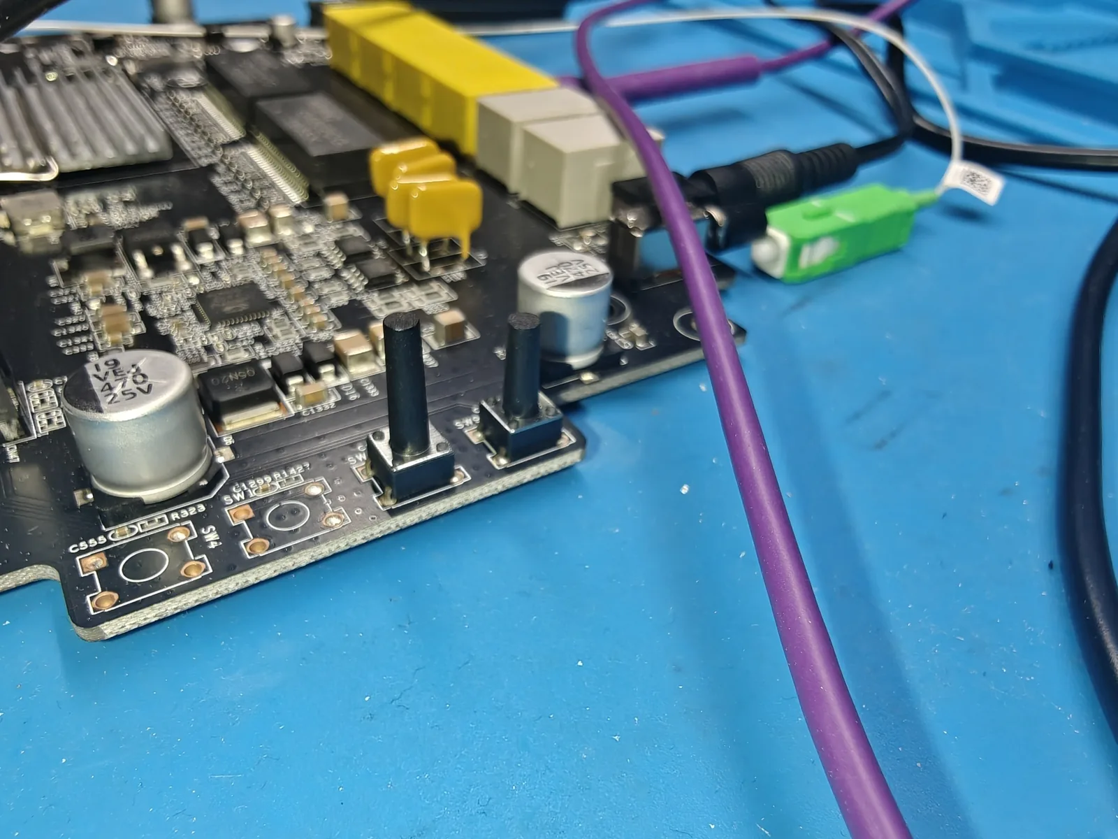
That left one final detail: the tactile push button on the right edge of the board (`SW8` / `SW9`) that maps to the `LED` button on the case.
The two populated long-stem tactile push buttons (SW8 and SW9, next to unpopulated footprints SW4 and SW10) on the right edge of the PCB, with the rear Gigabit LAN block, RJ-11 telephone jacks, DC barrel jack, and green SC/APC optical fiber connector in the background.
In the original Nokia firmware, pressing that button simply turned the status LEDs off. Instead, I wrote a small C daemon (`led_show.c`, started automatically at boot as `/usr/local/bin/led-show --daemon`) that monitors `GPIO 10` (`0x1fbf0204` bit 10) every 10 milliseconds:
- After booting into Linux, the board sits quietly with the green Power LED on.
- **Press the `LED` button**, and it kicks off the 9-pattern 13-LED dance show across the front panel.
- **Press the `LED` button again** at any point, and it stops the animation and goes back to the normal green Power LED.
---
## Code and Documentation
If you happen to have an old Nokia G-240G-E (or another EcoNet EN751221 board) lying around and want to try this yourself, or if you just want to browse the bootloader code, QEMU machine model, device trees, and Linux 7.4-rc1 patches, everything is up on GitHub:
- **GitHub Repository**: **[https://l.dj.vg/ont-code](https://l.dj.vg/ont-code)**